How to convert pcb to schematic diagram? Electronic devices & pcb development services — kickr design® Pcb layout connection kelvin smps supply power switch mode circuits properly given document also
Electronic Devices & PCB Development Services — Kickr Design®
Pcb diagram circuit layout convert step
Circuit diagram
Pcb layout design guidelines for switch mode power supply (smps) circuitsPcb disposition automatically footprints associated Pcb eda electrical pads mentor automation circuits easyeda autodesk verification tinycad expresspcb designspark vlsi autorouter indicators amplifier xpedition 2025 projectedSchematic eevblog.
Pcb layout electronic schematic engineering services reverse development packageMastering the art of pcb design basics Circuit diagram seekic connections external boardAnalog to digital converter circuit.

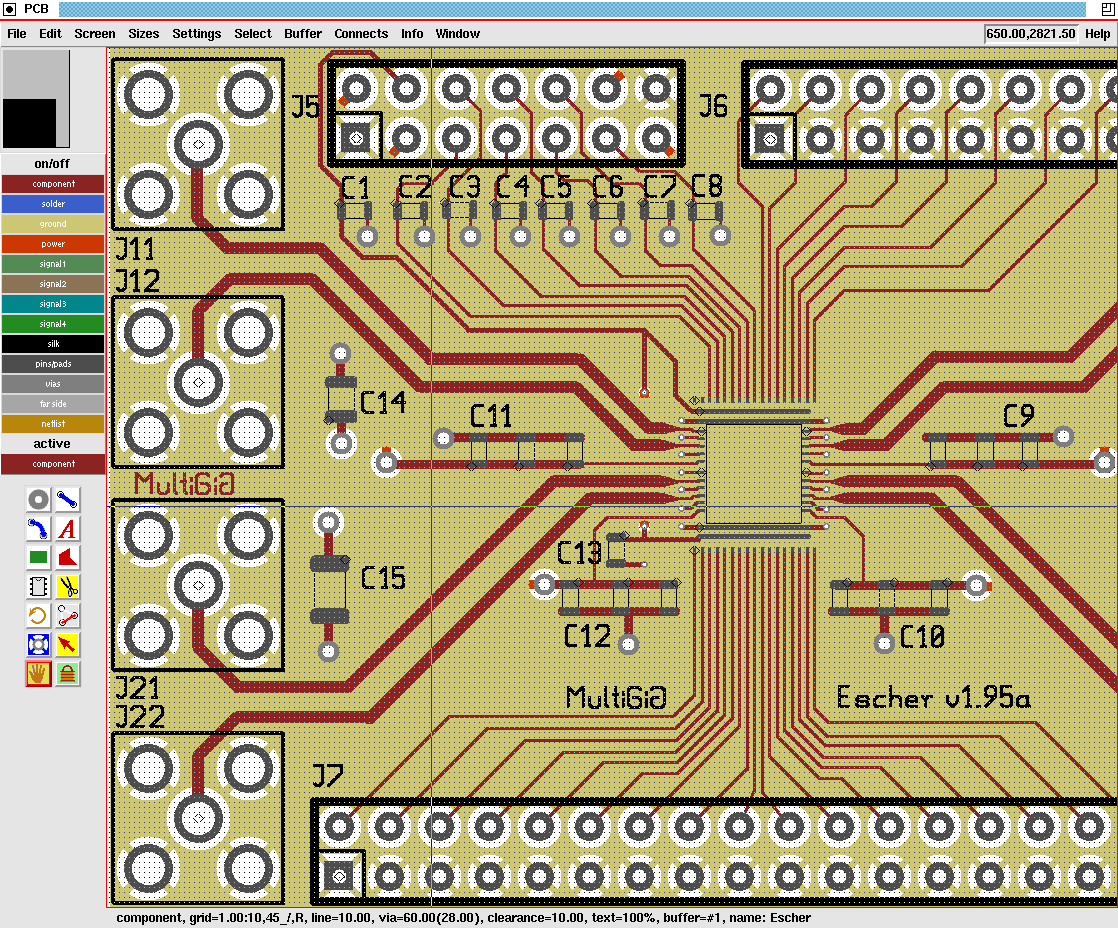
World technical: pcb version 3.0 printed circuit board layout tool
Pcb schematic make layout audio circuit custom amp startsHow to convert schematic diagram into pcb layout in easyeda online pcb How to convert pcb to schematic diagram?Pcb design.
Schematics according restore raypcb convert orcad protelHow to design a pcb layout How to design a pcb layoutSchematic diagrams compared other wiring layouts electrical engineering.

Circuit pcb diagram monostable diagrams understand layout drawn left board easier often follow some wizard which
My first pcb design, tell me what i've done wrong.Circuit diagram to pcb Pcb schematic diagram layout easyeda convert intoTop 10 free pcb design software for 2019.
Schematic diagram circuits basics mastering sierraPrinted circuit board design, diagram, assembly Dc converter circuit 555 boost gnd ne555 timer diagram using board ic circuits pcb supply step eleccircuit noise schematic 5vAnalog circuit converter digital schematic diagram simple pcb using layout parts actual sided copper single size components projects clock fig.

Rs485 rs232 converter circuit schematic layout power supply ttl rx tutorial airborn au pc board will pcb specification gif necessary
Schematic to pcb layout converterPcb circuit board printed version tcl layout tool screen technical based shot Pcb buck layout converter widths trace stack6 tips to ensure great pcb designs.
Pcb layout and trace widths for buck converter🔥🔥🔥 how to convert circuit diagram to pcb layout step by step 🔥🔥🔥 Converter pcb 220v 12vSchematic diagram.

Circuit diagram to pcb 2
.
.